Indium arsenide nanowires
Indium arsenide nanowires are a versatile platform for the experimental realization of nanocircuits. By tuning the electrostatic potential along the axis of the nanowire one can confine the conductance band electrons and form quantum dots (QD). By contacting the nanowire with different metallic electrodes, one can investigate the transport in normal-QD-normal, superconducting-QD-superconducting and ferromagnetic-QD-ferromagnetic structures. Apart from using the nanowires as building blocks, we also investigate their material properties via low-temperature electron transport, namely the strength of spin-orbit interaction and the electron g-factor.
Cooper pair splitting
The electronic ground state of a superconductor is composed of spin singlet electron pairs, so-called Cooper pairs. In a Cooper pair splitter nanocircuit two QDs are coupled to a superconducting lead, the Coulomb repulsion on the QDs force the incoming electron pairs to split and leave via opposite normal leads. The first succesful Cooper pair splitter realized in an InAs nanowire circuit had a splitting efficiency of a few percent. The efficiency was improved to approx. 30% by changing the device geometry and using a wide gap superconductor.
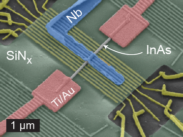
Scanning Electron Microscope image showing a representative sample of the first generation Cooper pair splitter devices [1].
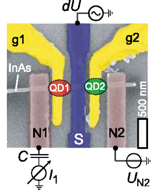
An advanced Cooper pair splitter device equipped with fine local finger gates. These allow us to tune the QD-electrode couplings, and utilizing them we have demonstrated the eletrical tuning of the nonlocal signal [2].
In magnetic field measurements we have shown that the CPS is a phase-coherent device, and the interference can strongly alter the nonlocal signal [3].
References
[1] Hofstetter L, Csonka S, Nygard J, Schonenberger C: Cooper pair splitter realized in a two-quantum-dot Y-junction, NATURE, 461, 7266 (2009)
[2] Fülöp G, d'Hollosy S, Baumgartner A, Makk P, Guzenko V A, Madsen M H, Nygård J, Schönenberger C, Csonka S: Local electrical tuning of the nonlocal signals in a Cooper pair splitter, PHYSICAL REVIEW B, 90, 23 (2014)
[3] Fülöp G, Domínguez F, d’Hollosy S, Baumgartner A, Makk P, Madsen M H, Guzenko V A, Nygård J, Schönenberger C, Levy Yeyati A, Csonka S: Magnetic Field Tuning and Quantum Interference in a Cooper Pair Splitter, PHYSICAL REVIEW LETTERS 115, Paper 227003 (2015)
Graphene
Graphene has many admirable qualities for applications, such as its strength, stability, optical and electronic properties. In the highest quality samples, electron trajectories are ballistic, which allows the fabrication of novel device configurations for the emerging field of electron optics. Moreover, the spin coherence length is uncommonly long, making graphene a useful material in future spintronics applications.
Graphene research at our lab has many branches:
- graphene nanoribbons (suspended or on substrate)
- graphene contacted with superconducting electrodes
- graphene on hexagonal boron nitride (hBN)
- ballistic transport in suspended or hBN-supported samples
Electron optics in suspended graphene
Clean, suspended graphene samples permit electrons to travel along ballistic trajectories. This means that the mean free path - the average distance an electron travels between collisions (with lattice defects, phonons, or impurities) that change its momentum - is larger than the sample size, which is on the micrometer scale. Different geometries of bottom gates make the realization of inhomogeneous doping along the same graphene flake, like p-n junctions, possible. On one side of a suspended graphene p-n junction current is carried by electrons, while on the other, holes, therefore, the group velocities are opposite. Recent research in collaboration with the Nanoelectronics Group of the University of Basel has shown that by applying a perpendicular magnetic field, the curved ballistic trajectories will snake along this p-n junction since the direction of the Lorentz-force is opposite on the two sides. This effect was observed in the conductance of the sample [1].
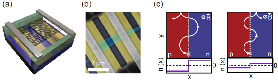
(a) Schematic view and (b) false-color SEM image of a graphene strip (black/cyan) suspended above two bottom gates (gold) capable of creating a p-n junction. [2] (c) Schematic of a charge trajectory (white) starting from a single point (grey cross) in a perpendicular magnetic field B, at different values of antysimmetrically set charge carrier density n(x) on the p and n sides. Depending on the radius of the half circles, current from left to right contacts (grey in (a) and (b) ) is either decreased (left panel: scattering to the left at the upper edge) or increased (right panel). [1]
Confinement in a magnetic field
The micrometer-scale spin coherence length in graphene makes it a promising candidate for spintronics and quantum computing applications. The latter requires electrons to be confined - in so-called quantum dots - to operate as quantum bits. Bulk graphene lacks a band gap, which hinders confinement, however, in a magnetic field, the band structure reforms into a series of Landau levels (LLs). When the Fermi energy is between two LLs, propagating states carry current along the edge, but the bulk of the device is insulating, and an external electrostatic potential can be used to achieve confinement.
We have observed conductance fluctuations in suspended graphene devices near the edges of quantum Hall plateaus [3], which can be explained by charging effects of quantum dots in the device. Here, quantum dots are formed due to a disorder potential from fabrication residues. They can also be interpreted as localized edge states in potential valleys (or hills, in the case of holes), confined due to the mechanism described above.
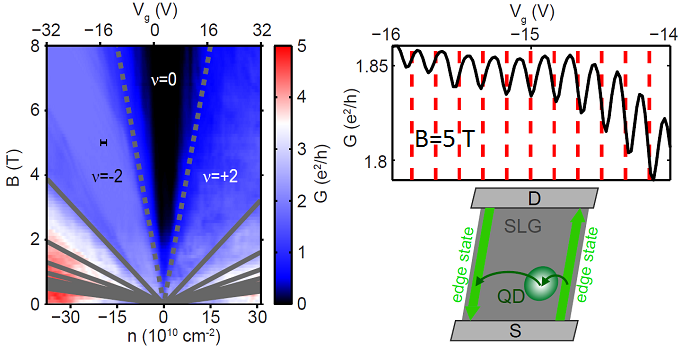
Regular fluctuations were observed in graphene nanoribbons near quantum Hall plateaus due to a single quantum dot causing scattering events between edge states (as drawn in the schematic), or between contacts. [3]
Our measurements provide a proof of concept for a confinement mechanism in single-layer graphene using a magnetic field, which makes the fabrication of devices such as quantum point contacts, quantum dots and interferometers possible.
Quantum Hall Channels (QHCs)
We have demonstrated [5] that the above mechanism can be realized in practice by using artificial electrostatic potentials: for instance, a quantum Hall propagating state have been localized using gate electrodes only. Though charging effects could not be observed due to its macroscopic size, the conductance contribution of this channel, circulating in the bulk of a bilayer graphene sample, have been observed, and its coupling to contacts has been controlled with gate voltages.
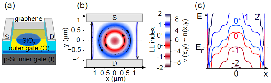
(a) Schematic of a double-gated device. (b) Filling factor map of the measured (bilayer graphene) sample based on electrostatic simulations: the circulating QHCs increase the conductance of quantum Hall plateaus, since they contribute to transport between source (S) and drain (D) contacts. (c) Schematic of Landau levels along the horizontal dashed line in (b): QHCs propagate at the intersections of Fermi energy and Landau levels. [5]
Electrostatic control of QHCs in graphene opens the way to fabricating similar devices to those already created in semiconductor 2D electron systems. Furthermore, our results enables the study and exploitation of spin or valley-polarized, or fractional QHCs, and also the quantum valley Hall effect, by directing channels into the bulk, avoiding disorder and valley decoherence at edges.
Electron optics in encapsulated graphene
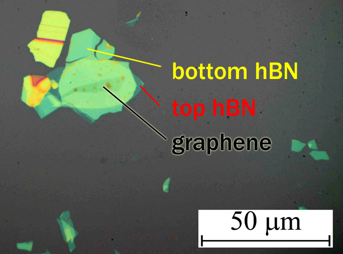
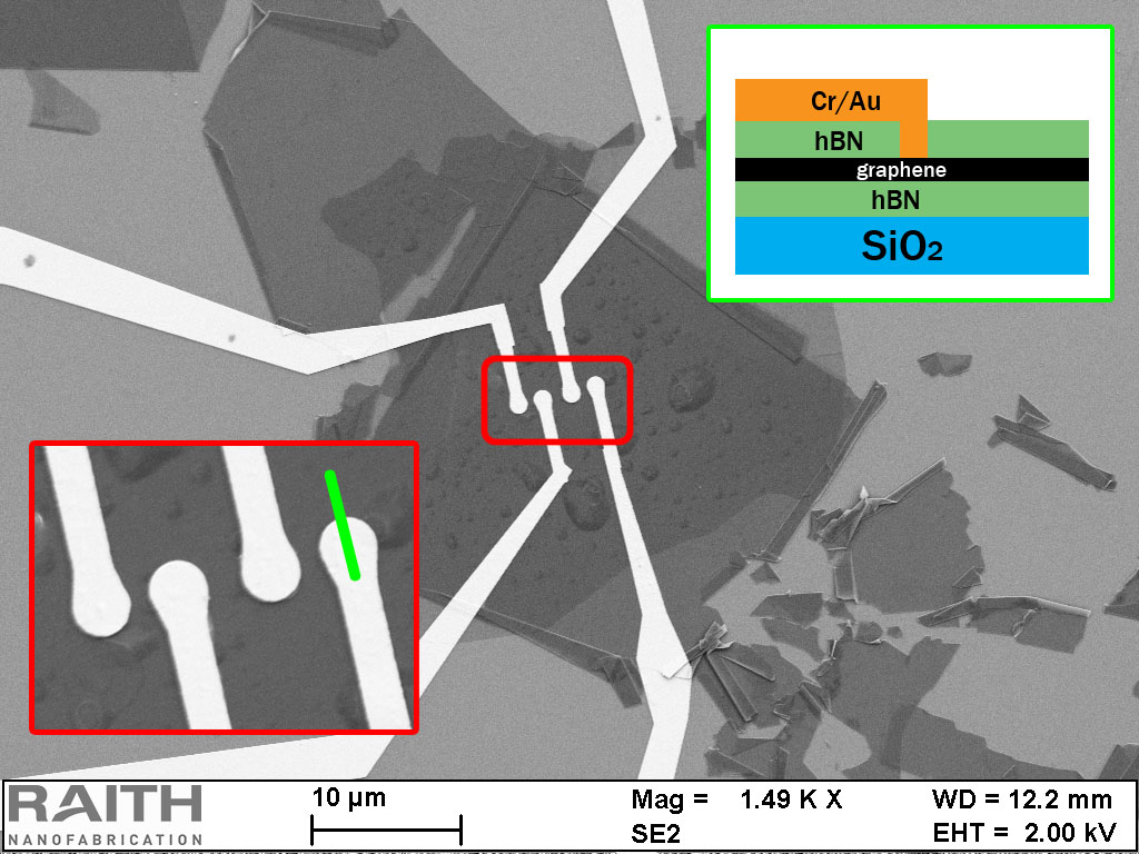
Another possible way to create clean graphene samples is to encapsulate it in hexagonal boron nitride (hBN) by following a dry-stacking assembly. This material has a quite similar structure to graphene but it is an insulator. The structural similarity leads to atomically clean adhesion between these layers and very high electrical performance. The picture below shows an example of a hBN-G-hBN stack on a SiO2 substrate in optical microscope.
In collaboration with the Dept. of Physics of University Basel we began to study these structures. Contrary to the conventional edge contacts of the graphene sheet it is also possible to create point-like contacts in the middle of the sheet by drilling holes in the top hBN flake prior to dry-stacking assembly.
2 and 4-terminal measurement results corroborate a 2D current flow model describing the behaviour of the current in the graphene flake assuming point-like electrical contacts in the middle of the flake. In high B-field the sample shows insulating behaviour which is expected by the quantum Hall effect in the case of isolated point contacts separated from each other.
References
[1] Peter Rickhaus, Péter Makk, Ming-Hao Liu, Endre Tóvári, Markus Weiss, Romain Maurand, Klaus Richter, Christian Schönenberger: Snake trajectories in ultraclean graphene p-n junctions, NATURE COMMUNICATIONS 6, Paper 6470 (2015)
[2] Maurand Romain, Rickhaus Peter, Makk Peter, Hess Samuel, Tovari Endre, Handschin Clevin, Weiss Markus, Schoenenberger Christian: Fabrication of ballistic suspended graphene with local-gating, CARBON 79, pp. 486-492 (2014)
[3] Endre Tóvári, Péter Makk, Peter Rickhaus, Christian Schönenberger, Szabolcs Csonka: Signatures of single quantum dots in graphene nanoribbons within the quantum Hall regime, Nanoscale 8, 11480 (2016)
[4] Handschin Clevin, Fülöp Bálint, Makk Péter, Blanter Sofya, Weiss Markus, Watanabe Kenji, Taniguchi Takashi, Csonka Szabolcs, Schönenberger Christian: Point contacts in encapsulated graphene, APPLIED PHYSICS LETTERS 107, Paper 183108 (2015)
[5] E. Tóvári, P. Makk, M.-H. Liu, P. Rickhaus, Z. Kovács-Krausz, K. Richter, C. Schönenberger, S. Csonka: Gate-controlled conductance enhancement from quantum Hall channels along graphene p-n junctions, Nanoscale 8, 19910 (2016)