Our central research objective is to establish and study novel device structures, where the characteristic size of the active region is close to atomic dimensions.
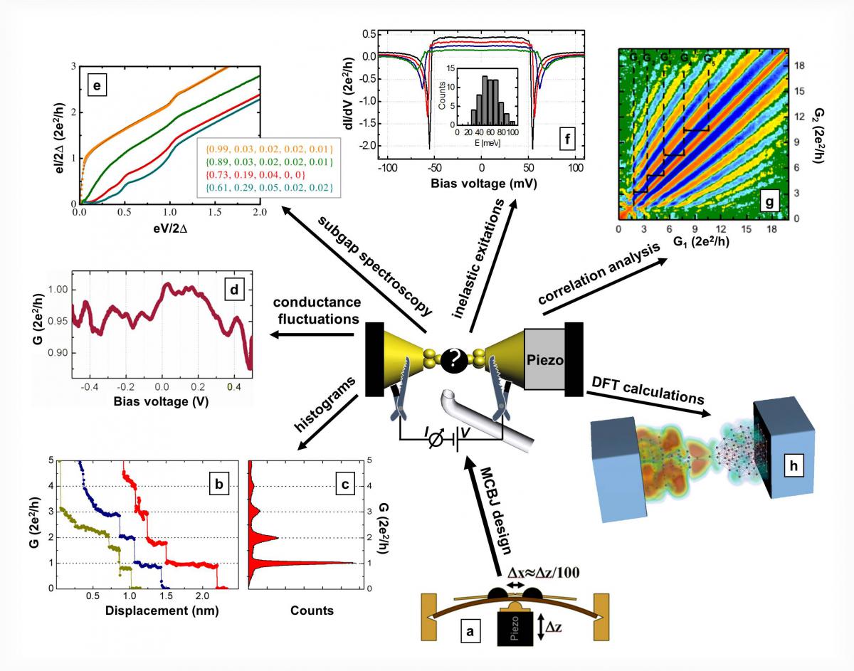
Our research group has long tradition in investigating single-atom and single-molecule conduction using the mechanically controllable break junction (MCBJ) technique. By mounting a metallic wire on the top of a bending beam and breaking the wire by the precise control of the bending one can investigate the final stage of the rupture, when the current flows through a single atom in the narrowest cross section (panel a). After the disconnection of the single-atom contact a sub-nanometer scale variable gap is established at the apex of the broken wire providing an ideal platform for contacting single molecules. Using this method several types of measurements can be performed, like the identification of single-atom or single molecule conductances by conductance histograms, the study of the transmission channels by superconducting subgap spectroscopy, the investigation of inelastic excitations by point-contact spectroscopy, or the study of junction evolution dynamics by advanced statistical methods (panels b-h).
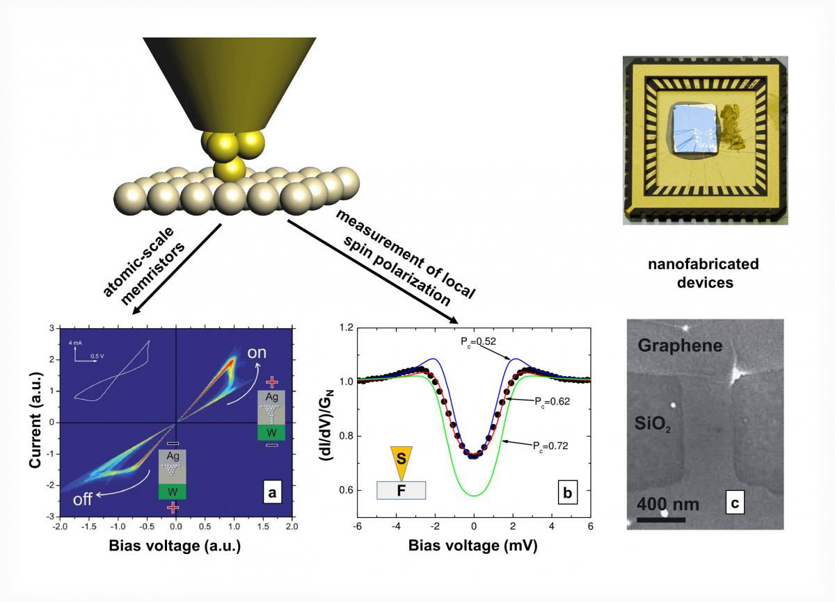
We have extended our experimental capabilities by building self-designed scanning tunneling microscope (STM) setups operating either at room temperature or at cryogenic circumstances. Whereas the MCBJ technique has superior stability to an STM, the STM setups enable the study of atomic-scale objects between two different electrode materials. Using this heterojunction geometry we focus on the study of atomic scale resistive switching memories (panel a), and the investigation of local, nanoscale spin polarization by Andreev spectroscopy (panel b).
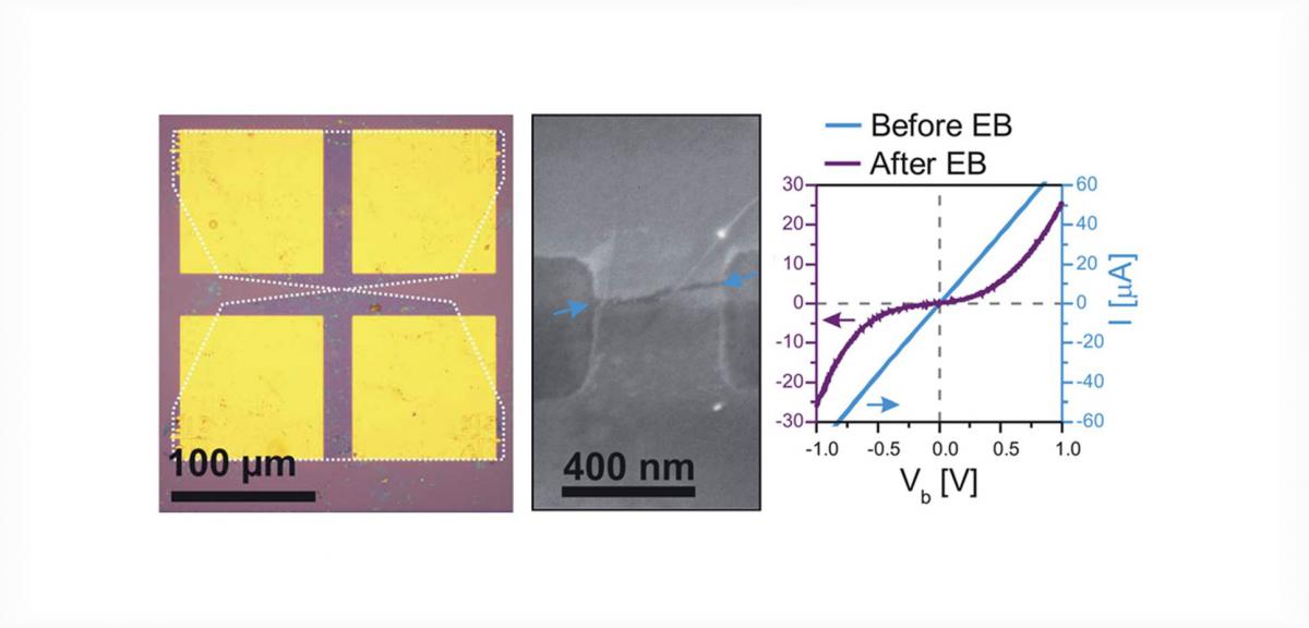
As a third platform we study nanocircuits predifiend by electron beam lithography, and thinned further to atomic dimensions by electromigration or electroburning techniques (panel c).
Some selected results:
Resistance-change memories
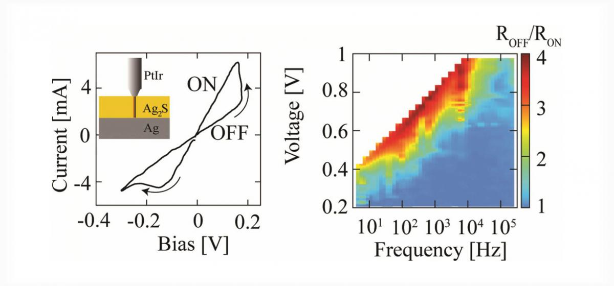
Tunable, nanometer scale Ag2S junctions formed between Pt and Ag electrodes are investigated in our group. We could initiate resistive switchings between metallic states with 500 ps pulses by varying the diameter of metallic filament from 2 to 5 nm. We showed that the resistance change simultaneously exhibits multiple time scales ranging from a nanosecond to seconds upon a switching voltage pulse. The resulting non-exponential transition between the OFF and ON states as well as the achievable, technologically convenient ROFF/RON = 2–10 ratios are largely affected by the amplitude and frequency of the biasing signals. This fundamental, inherent property of the Ag2S ionic conductor provides the unique opportunity for combination of GHz write/erase operations performed at bias levels of a few Volts, non-volatile read-out with slower signals of a few 10 mV and robust information storage at zero bias in a two-terminal, nanometer scale analog memory device.
A. Gubicza, D. Zs. Manrique, L. Pósa, C. J. Lambert, G. Mihály, M. Csontos, A. Halbritter, SCIENTIFIC REPORTS (2016)
A. Gubicza, M. Csontos, A. Halbritter, G. Mihály, NANOSCALE (2015)
A. Gubicza, M. Csontos, A. Halbritter, G. Mihály, NANOSCALE (2015)
A. Geresdi, M. Csontos, A. Gubicza, A. Halbritter, G. Mihály, NANOSCALE (2014)
A. Geresdi, A. Halbritter, E. Szilágyi, G. Mihály, MATERIALS RESEARCH SOCIETY SYMPOSIUM PROCEEDINGS (2011)
A. Geresdi, A. Halbritter, A. Gyenis, P. Makk, G. Mihaly, NANOSCALE (2011)
Interaction of carbon monoxide molecules with single-atom contacts and atomic chains
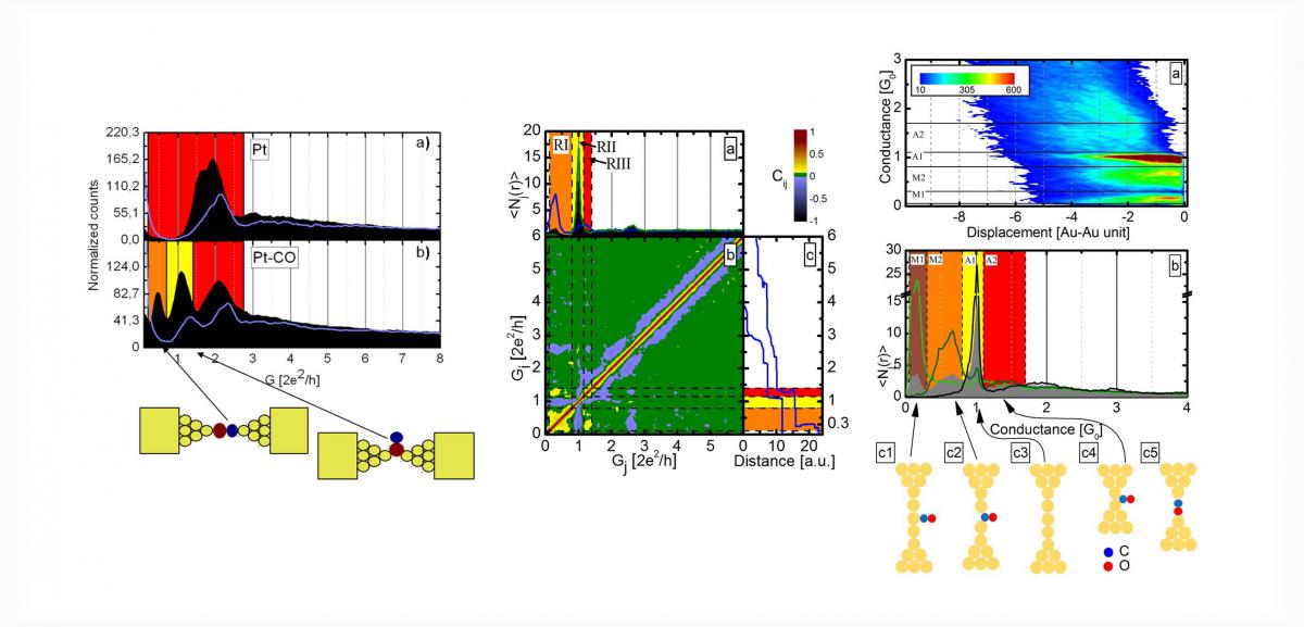
We have investigated the interaction of the carbon-monoxide molecule and different electrodes (Pt, Ag, Au) using the self-designed low temperature molecular measurement system. In these measurements the evolution of different molecular configurations were observed using comprehensive statistical analysis. These include rotations between perpendicular and parallel molecular orientation in the junction, the formation of very long molecule decorated chains and conductance reduction due to a Fano-like destructive interference effect in the atop geometry.
Z. Balogh, P. Makk, A. Halbritter, BEILSTEIN JOURNAL OF NANOTECHNOLOGY (2015)
Z. Balogh, D. Visontai, P. Makk, K. Gillemot, L. Oroszlány, L. Pósa, C. Lambert, A. Halbritter, NANOSCALE (2014)
P. Makk, Z. Balogh, S. Csonka, A. Halbritter, NANOSCALE (2012)
Nanometer-sized gaps in CVD graphene
In collaboration with the group of M. Calame at the University of Basel we demonstrated the controlled and reproducible fabrication of sub-5 nm wide gaps in single-layer graphene electrodes. The process is implemented for graphene grown via chemical vapor deposition using an electroburning process at room temperature and in vacuum. A yield of over 95% for the gap formation is obtained. This approach allows producing single-layer graphene electrodes for molecular electronics at a large scale.
C. Nef, L. Pósa, P. Makk, W. Fu, A. Halbritter, C. Schönenberger, M. Calame,, NANOSCALE (2014)
Correlation analysis of atomic and single-molecule junction conductance
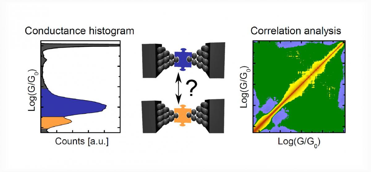
We have developed a novel statistical method based on the cross-correlation analysis of conductance traces. This method is capable of resolving several features of nanocontact formation dynamics, which are completely hidden in traditional conductance histograms, including the correlated and anticorrelated occurrence of different junction configurations, and the resolution of fine structures which are obscured in the histogram by random variations of the conductance. With this method we have discovered robust structures in the correlation diagrams of Ni, Fe and V contacts, which demonstrate a very regular atomic narrowing of the junction, in contrast to the rather unordered rupture of Au nanowires.
A. Magyarkuti, K.P. Lauritzen, Z. Balogh, A. Nyáry, G. Mészáros, P. Makk, G.C. Solomon, A. Halbritter, arXiv.org, (2016)
SV. Aradhya, M. Frei, A. Halbritter, L. Venkataraman, ACS NANO, (2013)
P. Makk, D. Tomaszewski,J. Martinek, Z. Balogh, S. Csonka, M. Wawrzyniak, M. Frei, L. Venkataraman, A. Halbritter, ACS NANO (2012)
A. Halbritter, P. Makk, S. Mackowiak, S. Csonka, M. Wawrzyniak, J. Martinek, PHYSICAL REVIEW LETTERS (2010)
Investigation of transmission channels by subgap spectroscopy
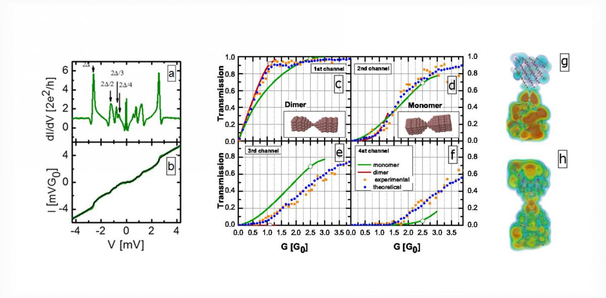
We have investigated the opening of conductance channels in atomic and molecular contacts by superconducting subgap method. Subgap structure measurements give a unique opportunity for the full determination of transmission probabilities for all the conductance channels, and the evolution of the channel transmission as a function of total conductance is characteristic of the studied system, providing significantly more information than the conductance histogram alone.
P. Makk, D. Visontai, L. Oroszlany, DZ. Manrique, S. Csonka, J. Cserti, C. Lambert, A. Halbritter, PHYSICAL REVIEW LETTERS (2011)
P. Makk, S. Csonka, A. Halbritter, PHYSICAL REVIEW B CONDENSED MATTER AND MATERIALS PHYSICS (2008)
Measurement of local, nanoscale spin polarization
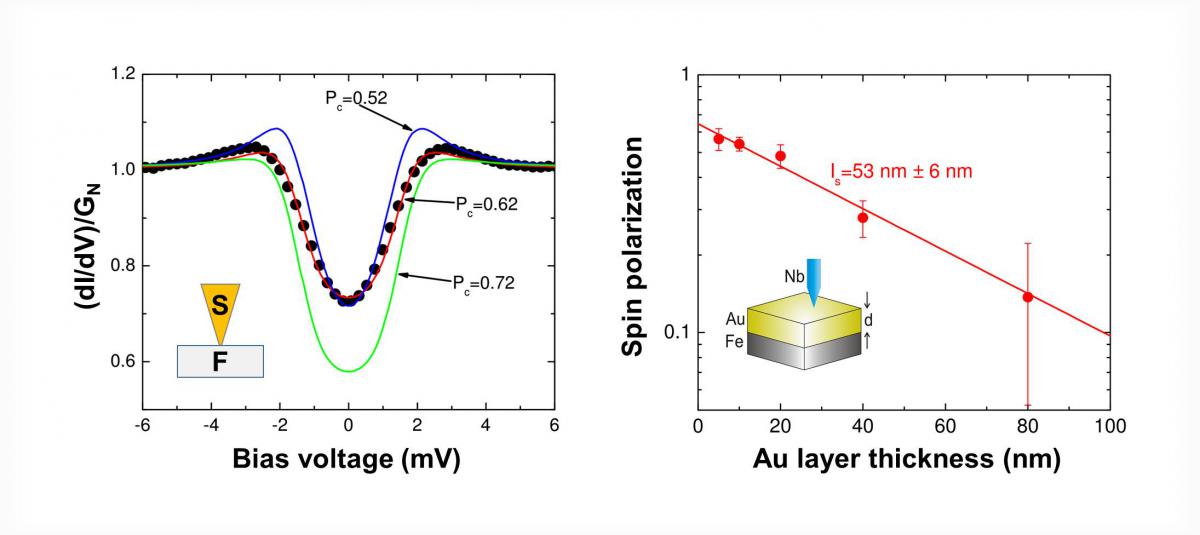
We investigated the local, nanoscale spin polarization by means of point contact Andreev reflection measurements, demonstrating that this method is capable of determining the spin diffusion length in ferromagnet/normal metal thin film structures. We have also demonstrated the presence of local magnetism well above the bulk Curie temperature of (In,Mn)Sb magnetic semiconductors.
A. Geresdi, A. Halbritter, F. Tancziko, G. Mihaly, APPLIED PHYSICS LETTERS (2011)
A. Geresdi, A. Halbritter, M. Csontos, S. Csonka, G. Mihály, T. Wojtowicz, X Liu, B. Jankó, JK. Furdyna, PHYSICAL REVIEW B CONDENSED MATTER AND MATERIALS PHYSICS (2008)
Huge negative differential conductance
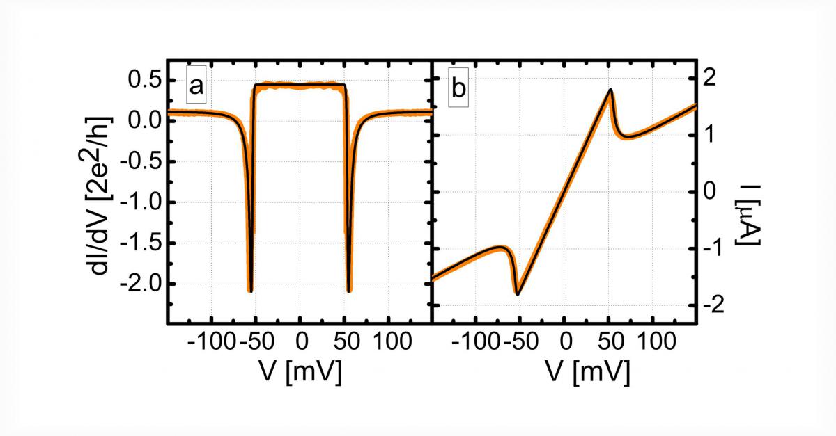
We have shown that I-V characteristics of molecular nanojunctions frequently show huge nonlinearities, even negative differential conductance due to the excitation of a strongly bound molecule to a large number of energetically similar loosely bound states.
A. Halbritter, P. Makk, S. Csonka, G. Mihály, PRB (2008)
A. Halbritter, L. Borda, A. Zawadowski, ADVANCES IN PHYSICS (2004)